


一维光子微腔结构多设计为法布里⁃珀罗(Fabry⁃Pérot,F⁃P)腔,主要用金属与介质膜来实现[12-14].和金属⁃介质型F⁃P腔相比,全介质型F⁃P腔由于具有更低的吸收、更好的调控能力和更高的选择透射率而备受青睐[15-17],且硅基材料是半导体器件及集成电路芯片中最重要的材料,有成熟的半导体工艺技术作为支撑.但半导体硅材料带隙较低(1.1 eV),对于常工作在可见光波段的光子器件的吸收系数较大,无法达到器件要求.而对于热光伏应用,由于辐射器的温度可能在1000~1500 K,发出的辐射波长在1.1~2.0
1 实验部分
1.1 原 料
通过等离子体增强化学气相沉积(PECVD)法在石英衬底以及p型硅衬底上生长了具有不同N/Si比和O/Si比的氮化硅(SiNx)和氮氧化硅(SiNyOz)薄膜,气源是纯度为99.999%的SiH4,N2O和NH3.
1.2 实验步骤
1.2.1 不同原子比的氮化硅(SiNx)和氮氧化硅(SiNyOz)薄膜的制备
为了对N/Si比和O/Si比进行调控,保持SiH4流量为5 sccm,在制备氮化硅(SiNx)薄膜时,改变NH3的流量为2.5,5,10,20 sccm;在制备氮氧化硅(SiNxOy)薄膜时,改变N2O的流量为5,20,40,80 sccm.以上不同样品以气流比
1.2.2 SiNx/SiNyOz微腔结构的制备与性能表征
通过对单层薄膜的透射谱和能量色散X⁃射线光谱(EDS)分析,得到不同生长参数下薄膜的折射率、原子比和生长速率等性质,再交替生长特定厚度的微腔结构.基于时域有限差分法建立微腔结构模型,根据实验得到的折射率等参数进行模拟计算.由于石英衬底对样品的透射性质影响极小,在建模中使用300 nm的SiO2作为衬底材料,所用氮化硅及氮氧化硅的折射率分别设置为2.67和1.62,计算得到微腔结构的透射谱.进而使用SHIMADZU UV⁃3600Plus分光光度计对多层膜样品的光吸收特性进行测量,并得到样品的透射谱.
2 结果与讨论
2.1 材料特性分析
图1
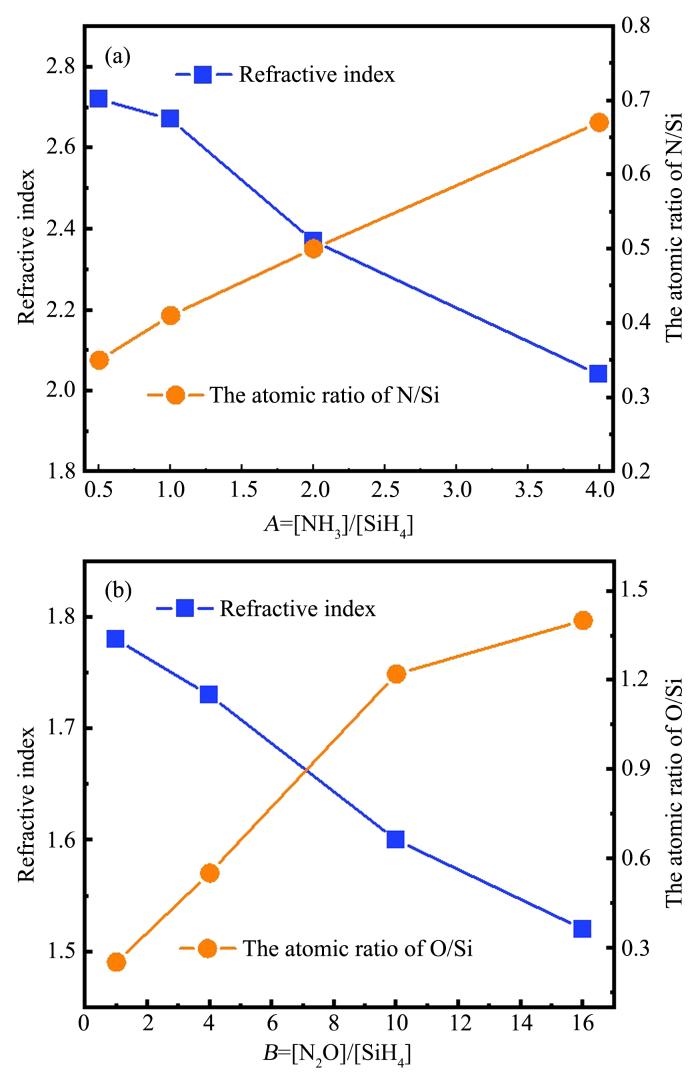
图1
(a) a⁃SiNx的折射率和Si/N原子比随
Fig.1
(a) a⁃SiNx's refractive index and Si/N atomic ratio with different ratio of
2.2 仿真模拟分析
为了研究基于非晶氧化硅和氮氧化硅材料的微腔特性,设计了三种结构进行了模拟研究.图2是三种结构的示意图.其中结构A在a⁃SiNyOz中间层两侧各有两个周期的DBR反射结构,而结构B有三个周期的反射结构,结构C则将高折射率的a⁃SiNx层作为最外层,也就是只有2.5个周期反射结构.两侧反射结构形成
图2
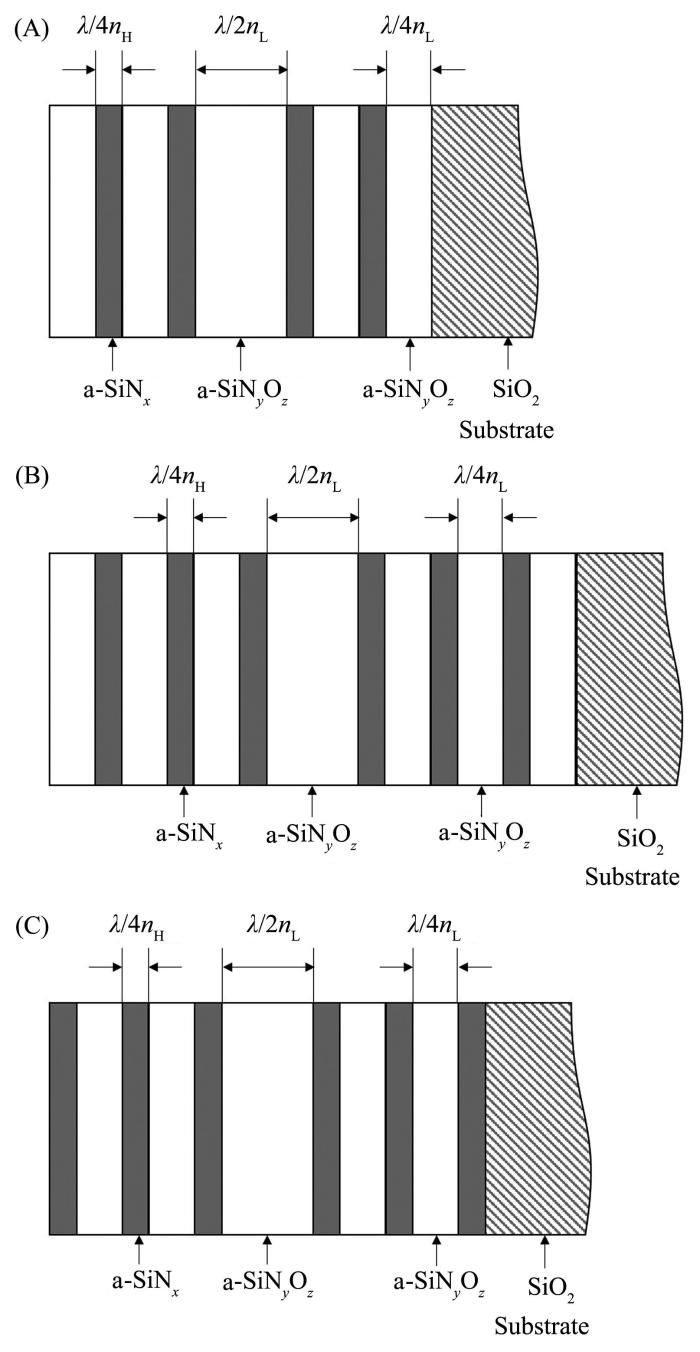
图2
三种微腔的剖面结构示意图
Fig.2
Schematic diagram of the cross⁃section structure of three microcavities
图3给出了对不同结构微腔透射谱的模拟研究结果,其中图3a是具有不同结构A,B,C的微腔的模拟透射谱结果,中心波长设计在1.1
图3
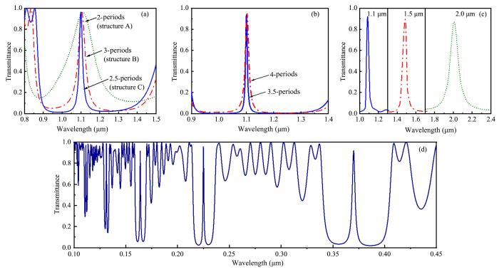
图3
(a)分别具有2,2.5,3个反射周期的微腔的模拟透射谱;(b)分别具有3.5,4个反射周期的微腔的模拟透射谱;(c)中心波长分别为1.1,1.5和2.0 μm的结构C微腔的模拟透射谱;(d)中心波长为1.1 μm的结构C微腔在短波段的模拟透射谱
Fig.3
Simulated transmission spectra of microcavity with (a) 2, 2.5 and 3 reflection periods,(b) 3.5 and 4 reflection periods, respectively,simulated transmission spectra of structure C microcavities with (c) center wavelength of 1.1, 1.5 and 2.0 μm, respectively,(d) center wavelength of 1.1 μm in the short band
对于中心波长为1.1
图3c是基于结构C,通过改变设计的中心波长所得到的模拟结果,其中心波长分别为
2.3 实验表征分析
基于模拟研究结果选择结构C来制备全硅基微腔.考虑到在热光伏系统中,目前辐射调控的波段在1.1~2.0
图4
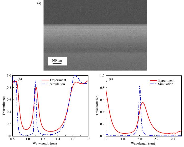
图4
中心波长为1.1
Fig.4
Microcavity with a center wavelength of 1.1 μm: (a) cross⁃section SEM photograph, (b) transmission spectrum obtained from simulation and experiment,(c) simulation and experimental transmission spectra of a microcavity with a center wavelength of 2.0 μm
图4c是对共振波长为2.0
2.4 讨 论
比较以上模拟得到的透射谱和实际制备样品得到的透射谱,发现样品的透射谱与模拟结果并不能实现完美的匹配,仍然存在误差.首先,样品的透射峰相对于模拟透射峰有所偏移,这是因为在PECVD生长过程中,对速率和时间的控制无法完全精确,导致薄膜的实际厚度与设计的理想厚度有偏差.从图4a的扫描电镜照片可以看到生长的薄膜总厚度大于设计厚度,这使样品的透射谱的峰值向长波方向移动.同时,每一层薄膜厚度的偏差也会导致样品的透射峰变宽,因为两侧厚度不完美的DBR膜系会降低F⁃P腔的窄带滤波特性,引起透射峰值两侧较大波长范围的透过,使得半高宽变大.
在模拟研究中没有考虑薄膜的吸收,为了探讨材料吸收对微腔性质的影响,进一步模拟具有不同消光系数(复折射率的虚部)的材料来构成微腔.图5a代表a⁃SiNx膜在1.1
图5
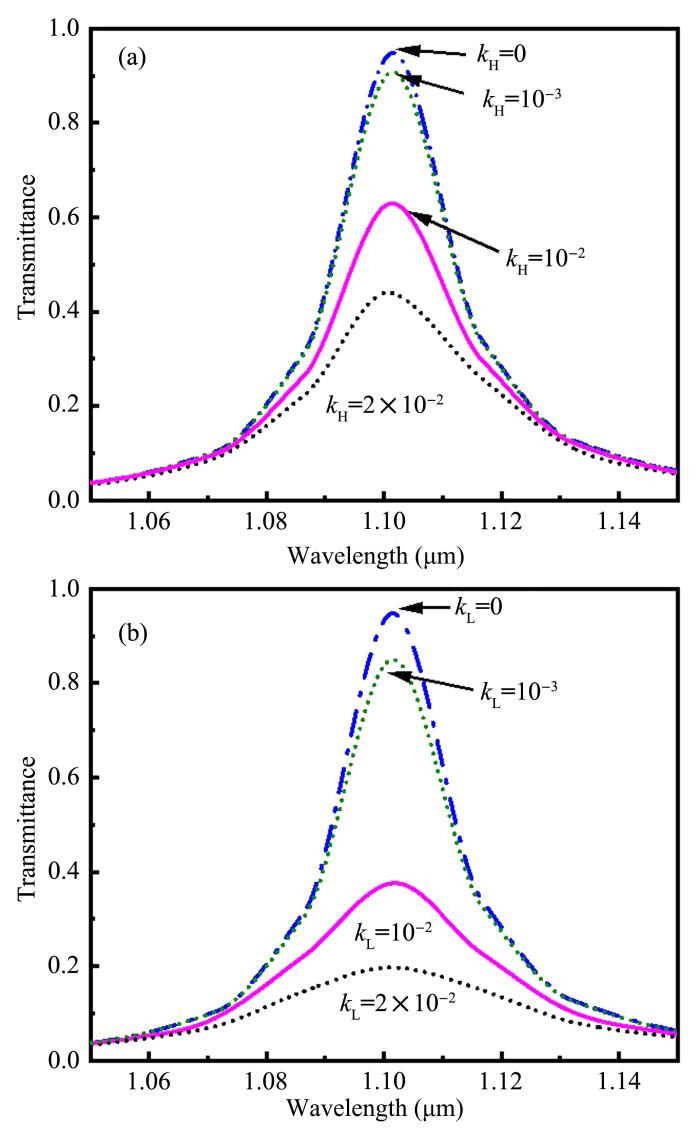
图5
(a)假设氮氧化硅材料消光系数(kL)为0时,改变氮化硅的消光系数(kH)为
(b) when kH is 0, the simulated transmission spectrum with different kL of
Fig.5
(a) When kL is 0,the simulated transmission spectrum with different kH of
3 结 论
本文研究了全硅基介质膜微腔结构,由实验得到的a⁃SiNx和a⁃SiNyOz的光学参数,通过模拟研究了不同结构的微腔透射特性.发现将反射层的最外侧设计为高折射率膜可以得到性能较好的微腔效应.进而利用PECVD制备了相应的全硅基介质膜微腔样品.针对在热光伏中的应用要求,将共振选择波长定为1.1
参考文献
Optical fiber fiber fabry–perot filter with tunable cavity for high–precision resonance wavelength adjustment
金属等离子激元调控Fabry–Perot微腔谐振模式研究
Resonant mode of Fabry–Perot microcavity regulated by metal surface plasmons
Plasmon–enhanced ultraviolet photoluminescence from the hybrid plasmonic Fabry–Perot microcavity of Ag/ZnO microwires
Analysis and numerical simulation of a novel optical microcavity with the roof structure
Performance analysis of solar thermophotovoltaic conversion enhanced by selective metamaterial absorbers and emitters
Solar thermophotovoltaics:progress,challenges and opportunities
10% efficiency solar thermophotovoltaic systems using spectrally controlled monolithic planar absorber/emitters
∥
Enhanced photovoltaic energy conversion using thermally based spectral shaping
Spectrally selective solar absorber with sharp and temperature dependent cut–off based on semiconductor nanowire arrays
Experimental testing of SiNx/SiO2 thin film filters for a concentrating solar hybrid PV/T collector
Tunable narrowband mid⁃infrared thermal emitter with a bilayer cavity enhanced Tamm plasmon
Reflective color filters and monolithic color printing based on asymmetric fabry–perot cavities using nickel as a broadband absorber
Fabrication of FP–cavity⁃based monolithic full–color filter arrays using a template–confined micro–reflow process
Microscopic interference full–color printing using grayscale–patterned fabry–perot resonance cavities
New development of one–dimensional Si/SiO2 photonic crystals filter for thermophotovoltaic applications
Optimization of spectrally selective Si/SiO2 based filters for thermophotovoltaic devices
Wide bandwidth and high resolution planar filter array based on DBR–metasurface–DBR structures
Planar light–emitting microcavities based on hydrogenated amorphous silicon carbide
Luminescence behavior from amorphous silicon–carbide film–based optical microcavities
Broadband mid⁃infrared frequency comb generation in a Si3N4 microresonator
氮氧化硅薄膜的光学特性及其在光波导中的应用
∥
Optical properties of silicon oxynitride films and their applications in optical waveguides
∥
